IMPORTANT NOTE: I have mentioned this already in the previous tutorials but I will repeat it in every LPC1768 Tutorial. Download both the Datasheet and User Manual for LPC1768 MCU from the official NXP website. I cannot explain / discuss each and every topic in detail. You have to look up for the topic of discussion in those documents and gather additional information.
Introduction
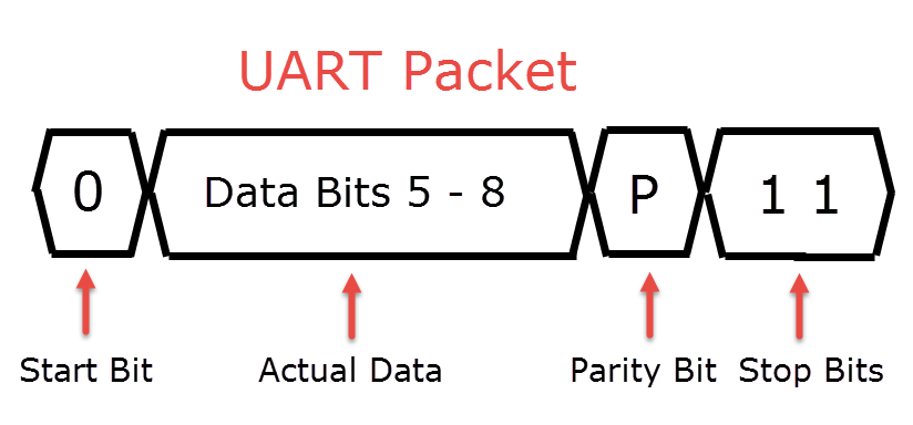
UART is short for Universal Asynchronous Receiver / Transmitter. It is a type of serial communication usually between a Microcontroller and a Computer. UART is a full-duplex communication and hence it needs two wires/lines between the communicating devices. They are called as TX and RX. The ‘A’ in UART stands for Asynchronous. What this means is that there is no clock signal between the communicating devices (in contrast to I2C and SPI, which are also Serial Communications but use a clock signal to synchronize data). Another important thing to know about UART Communication is how the data is transmitted. In UART, the data is transmitted in the form of ‘packets’ or ‘frames’. The structure of a typical UART data packet is shown below.
At the beginning of a frame, there is START Bit, which is a ‘0’ and it indicates the receiver about the data about to be transmitted. The START Bit is followed by the actual data to be transmitted. Its length can be anywhere between 5-bits and 8-bits. After the data, there is a parity bit, which can be used for error checking. This bit is optional. Finally, to signify the end of current data transfer, there are STOP Bits, which is usually ‘1’ of length 1 or 2 bits wide. To transmit the next set of data, repeat the process.
UART in LPC1768
Coming to UART in LPC1768 MCU, it consists of four UART peripherals viz.
UART0 UART1 UART2 UART3
UART0, UART2 and UART3 are identical with basic UART functionality, while UART1 adds full modem control handshaking support. Additionally, UART1 also supports RS-485. The UART0 is used for in-system programming. Both UART0 and UART1 are enabled after reset.
Pins Associated with UART
Since UART need two pins for communication i.e. TXD and RXD, the following table describes the pins that are mapped to all the UART peripherals. Note that some UART pins are mapped to multiple pins.
UART Pins Mapped to TXD Pins Mapped to RXD UART0 P0.2 P0.3 UART1 P0.15 / P2.0 P0.16 / P2.1 UART2 P0.10 / P2.8 P0.11 / P2.9 UART3 P0.0 / P0.25 / P4.28 P0.1 / P0.26 / P4.29
NOTE: For UART1, there are additional pins related to Hardwar Flow Control.
Architecture of UART in LPC1768
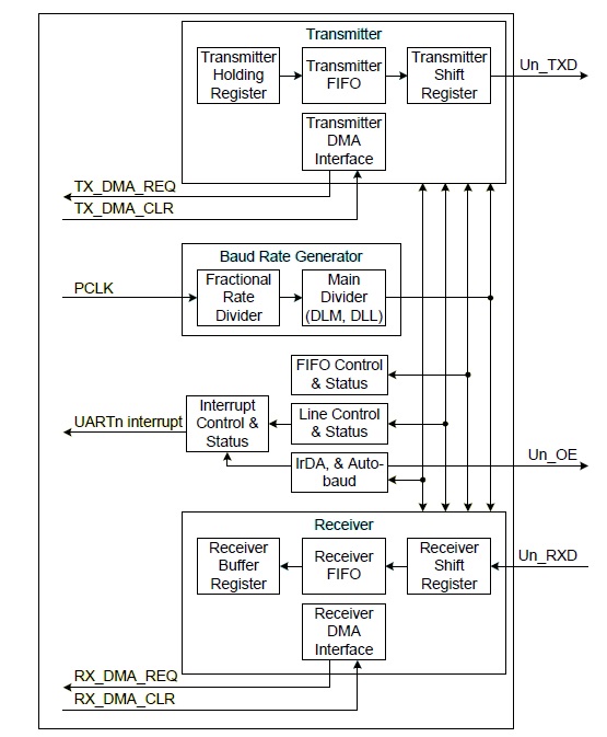
The following image shows the block diagram of the UART Peripheral in LPC1768. Both the Transmitter and the Receiver blocks contain 16 Byte FIFOs to hold the outgoing and incoming data respectively.
In case of data transmission, the data to be transmitted is written into the THR Register. This data is then buffered into the TX FIFO. A shift register then reads the data from the buffer and transmits is via the corresponding TXD Pin. Coming to receiving data, a valid data is captured by the shift register in the receiver block and is transmitted to the RX FIFO. Finally, the data is held in the RBR register for the processor to access it.
LPC1768 UART Registers
UART0, UART2 and UART3 have 14 registers each for UART Data, Interrupt, Status and Control. UART1 has a total of 18 registers. Let me explain some of the important registers of UART0/2/3.
NOTE: I am going to use the nomenclature from the reference manual for explaining UART Registers. For example, when I say UxRBR, it represents the Receiver Buffer Register of either UART0, UART2 or UART3 i.e. x = 0 or 2 or 3.
UxFCR – FIFO Control Register: Controls the UARTx RX and UARTx TX FIFO operations.
Bit 0 FIFO Enable When 0, FIFOs are disabled. When 1, both RX and TX FIFOs are enabled. Bit 1 RX FIFO Reset When 1, the RX FIFO will be cleared and reset. Bit 2 TX FIFO Reset When 1, the TX FIFO will be cleared and reset. Bits [7:6] RX Trigger Level Used to determine that how many RX FIFO characters must be written before an interrupt or a DMA request is activated.
UxLCR – Line Control Register: Determines the data format used in transmission.
Bits [1:0] Word Length Select When [00], 5-bit character length. Similarly [01], [10] and [11] for 6, 7 and 8-bit character lengths respectively. Bit 2 Stop Bit Select When 0, 1 stop bit and when 1, 2 stop bits. Bit 3 Parity Enable When 0, Parity generation & checking is disabled. When 1, it is enabled. Bit [5:4] Parity Select When [00], Odd parity. Similarly, for [01], [10] & [11], Even Parity, Forced “1” stick parity & Forced “0” stick parity respectively. Bit 6 Break Control When 0, disable break transmission. 1 to enable it. Bit 7 Divisor Latch Access Bit (DLAB) When 0, disable access to Divisor Latches. 1, to enable it.
UxLSR – Line Status Register: Provides the status of RX and TX blocks.
Bits 1 to 4 get cleared after reading UxLSR.
Bit 0 Receiver Data Ready (RDR) When 0, UxRBR is empty. When 1, UxRBR contains valid data. Bit 1 Overrun Error (OE) Over run is a condition when RSR (receiver Shift Register) has a new character assembled but the RBR FIFO is full. In this case, the RBR FIFO will not be overwritten and the character in the UARTx RSR will be lost. When 1, Overrun has occurred. Bit 2 Parity Error (PE) When 1, parity error has occurred. A parity error occurs when the parity bit in the received character is in wrong state. Bit 3 Framing Error (FE) When 1, framing error has occurred. Framing error occurs when the stop bit of a received character is 0. Bit 4 Break Interrupt When 1, break interrupt has occurred. Bit 5 Transmit Holding Register Empty (THRE) When 0, UxTHR contains valid data. When 1, UxTHR is empty. Bit 6 Transmitter Empty (TEMT) When 0, UxTHR and/or the UxTSR contains valid data. When 1, both are empty. Bit 7 Error in RX FIFO(RXFE) When 0, UxRBR contains no RX errors. When 1, UxRBR contains at least 1 error.
UxTER – Transmit Enable Register: Used to enable UART transmission. When TXEN (Bit 7) is set to 1, the TX block will keep on transmitting data as long as it is available. If TXEN is set to 0, then transmission will stop.
UxRBR – Receiver Buffer Register: This register contains the top byte of the RX FIFO i.e the oldest character received data in FIFO. Before reading from UxRBR, the DLAB (Divisor Latch Access) bit in UxLCR register must be 0.
UxTHR – Transmit Holding Register: UxTHR contains the top byte in TX FIFO. It is the newest character in the TX FIFO. The DLAB in UxLCR must be 0 in order to access UxTHR.
UxDLL and UxDLM – Divisor Latch Registers (LSB and MSB): These registers are a part of baud rate generator. Together, they contain the 16-bit divisor value for the APB Clock to generate the desired baud rate. UxDLL contains the lower 8-bits of the divisor while UxDLM contains the higher 8-bits. Before accessing these registers, the DLAB bit in UxLCR must be 1.
UxFDR – Fractional Divider Register: It controls the clock pre-scalar value for baud rate generation. The APB Clock is divided into a desired clock based of the divider and multiplier values in this register.
Bits [3:0] DIVADDVAL Pre-scalar divisor value. Bits [7:4] MULVAL Pre-scalar multiplier value. Minimum value is 1.
Baud Rate Calculation
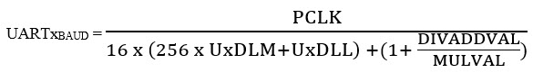
As per the reference manual of LPC1768 MCU, the following formula can be used to calculate the baud rate for UART0/2/3 peripherals.
This equation can be rearranged as follows:
Here,
PCLK is the Peripheral Clock in Hz MULVAL and DIVADDVAL are part of UxFDR register to set the clock pre-scalar UxDLL and UxDLM are baud rate divider values.
When choosing MULVAL and DIVADDVAL value, you must comply to the following rules:
1 ≤ MULVAL ≤ 15 0 ≤ DIVADDVAL ≤ 14 DIVADDVAL < MULVAL
Initializing UART
Let us now see how to initialize the UART0 Peripheral in order to set the following parameters:
PCLK: 25 MHz Baud Rate: 115200 Data Bits: 8 Stop Bits: 1 Parity: None
In order to get the baud rate of 115200, we have to use the following values:
U0DLL = 12 U0DLM = 0 MULVAL = 15 DIVADDVAL = 2
So, first set the UART0 TXD and RXD pins for UART Functionality in the PINSEL Register. LPC_PINCON->PINSEL0 |= (1«4) | (1«6); Since UART0 is enabled on reset, we do not have to configure it in the PCONP Register. Next, set the data frame using LCR Register. LPC_UART0->LCR = 3 | (1«7); Here DLAB bit is also set so that we can make changes to the DLL and DLM registers. We have to make DLAB as 0 once the DLL and DLM values are set. Now set the DLL and DLM values and enable the RX and TX FIFOs. LPC_UART0->DLL = 12; LPC_UART0->DLM = 0; LPC_UART0->FCR |= (1«0) | (1«1) | (1«2); In the FDR Register, set the MULVAL and DIVADDVAL values. After this, you can clear the DLAB Bit. LPC_UART0->FDR = (15«4) | 2; LPC_UART0->LCR &= ~(1«7); These steps will initialize the UART0 peripheral with the desired baud rate and data frame.
Example
Now, using the above initialization steps, let us write a program to transmit a set of characters (Hello) from LPC1768 MCU to a Computer’s Serial Terminal. #include <lpc17xx.h> #define THRE (1«5) #define MULVAL 15 #define DIVADDVAL 2 #define Ux_FIFO_EN (1«0) #define RX_FIFO_RST (1«1) #define TX_FIFO_RST (1«2) #define DLAB_BIT (1«7) #define CARRIAGE_RETURN 0x0D void UART0_Init(void); void UART0_Write(char data); int main(void) { char msg[] = { ‘H’,’e’,’l’,’l’,’o’,’\0′ }; int count=0; UART0_Init(); while(1) { while( msg[count]!=’\0′ ) { UART0_Write(msg[count]); count++; } UART0_Write(CARRIAGE_RETURN); count=0; } return 0; } void UART0_Write(char txData) { while(!(LPC_UART0->LSR & THRE)); LPC_UART0->THR = txData; } void UART0_Init(void) { LPC_PINCON->PINSEL0 |= (1«4) | (1«6); LPC_UART0->LCR = 3 | DLAB_BIT ; LPC_UART0->DLL = 12; LPC_UART0->DLM = 0; LPC_UART0->FCR |= Ux_FIFO_EN | RX_FIFO_RST | TX_FIFO_RST; LPC_UART0->FDR = (MULVAL«4) | DIVADDVAL; LPC_UART0->LCR &= ~(DLAB_BIT); }
Conclusion
A tutorial on how to UART in LPC1768 MCU. I have explained all the basic things like UART Pins, Registers, Baud Rate Generation, Initialization of UART and also an example program. Comment * Name * Email * Website
Δ
![]()
![]()
![]()

![]()
![]()

